Earlier quoted context omitted.
Not all densities is mass per volume. eg. population density.
It's a physical quantity per some unit of spatial measurement so the units still don't match up b/c in one case the transistors are stacked per volume & in the other case per area. > Historically, "node" sizes (like 28nm or 7nm) directly correlated to the physical length of a transistor's gate. Today, names like 3nm or 2nm reflect a marketing generation. The actual transistors are significantly larger than these nano…
IBM debuts sub-1 nanometer chip technology
201–210 of 217 posts
Re: IBM debuts sub-1 nanometer chip technology
#202Earlier quoted context omitted.
Why not use something absolute, like nand-gates per volume?
Transistor density in units of MTr/mm. (Million Transistors per square mm) is also used. The formula is MTr/mm = 0.6×(NAND2 Tr Count)/(NAND2 Cell Area) + 0.4×(Scan Flip Flop Tr Count)/(Scan Flip Flop Cell Area)
Re: IBM debuts sub-1 nanometer chip technology
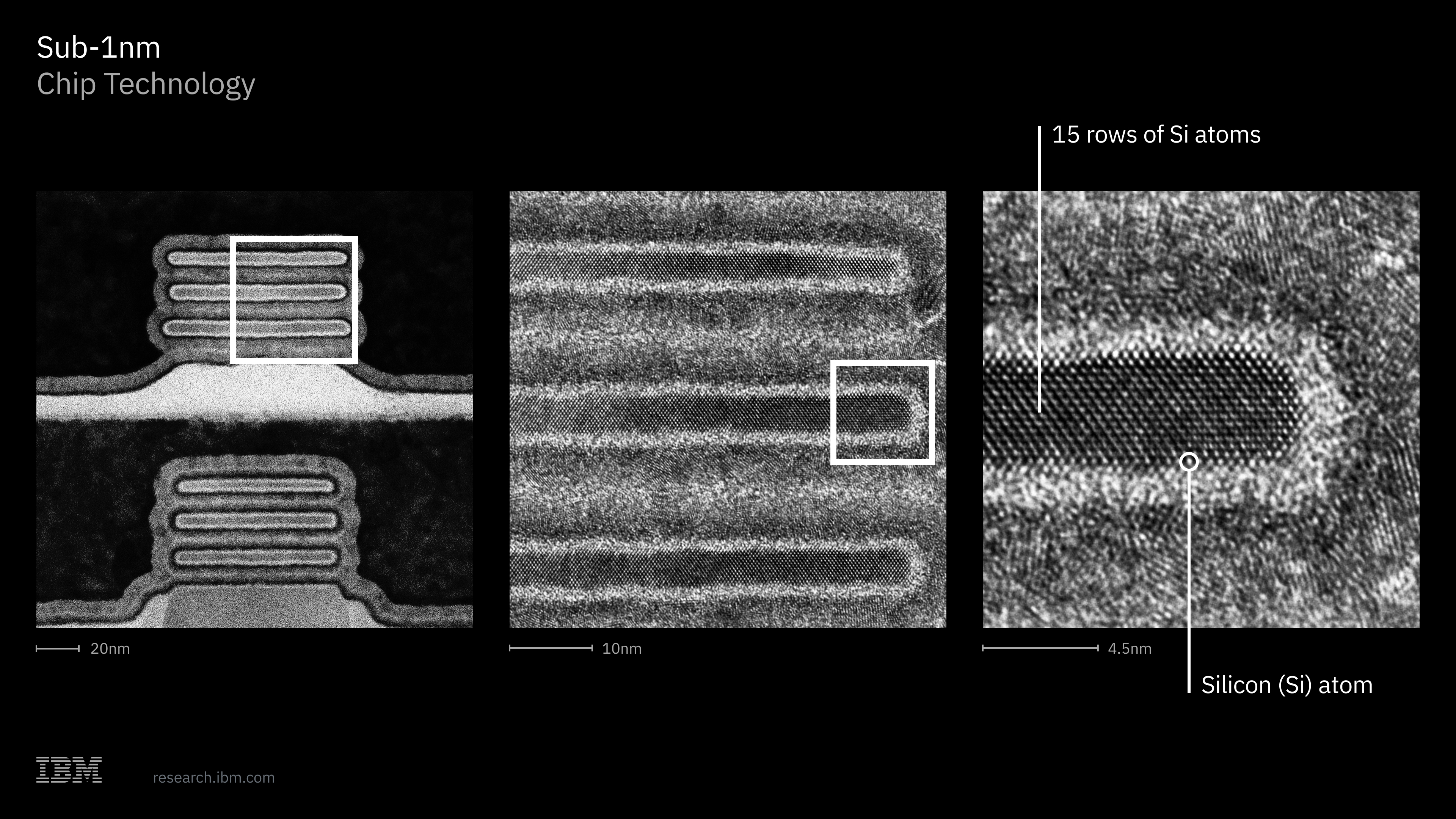
#203I am just astonished at the quality of the structure. Not only that, but the quality of the "cut" to then be able to take this picture. I was closely involved in EM imaging more than 30 years ago, this is just wonderful to see such pictures now.
Re: IBM debuts sub-1 nanometer chip technology
#204Earlier quoted context omitted.
It's a physical quantity per some unit of spatial measurement so the units still don't match up b/c in one case the transistors are stacked per volume & in the other case per area. > Historically, "node" sizes (like 28nm or 7nm) directly correlated to the physical length of a transistor's gate. Today, names like 3nm or 2nm reflect a marketing generation. The actual transistors are significantly larger than these nano…
The comparison is good. Humans are also stacked in volumes and we still measure population density over a surface because the third dimension is less significant in this context.
Re: IBM debuts sub-1 nanometer chip technology
#205Earlier quoted context omitted.
People love to hate on IBM, ask why it is relevant today, while several of their beloved FOSS projects are in some way, form or fashion, made possible with IBM's money.
which beloved FOSS were funded by IBM?
Re: IBM debuts sub-1 nanometer chip technology
#206> logic technology can extend for the first time below the 1 nm node, advancing the era of angstrom-level scaling, where dimensions approach the size of individual atoms. While transistor nodes now refer to a generation of manufacturing technology versus an exact physical dimension, IBM’s 0.7 nm technology—also referred to as 7 angstroms—demonstrates how continued scaling remains possible. Continuing the well establi…
It's been decades since published node sizes had any connection to actual feature size. Sadly this is just how it works in the semiconductor industry now.
Re: IBM debuts sub-1 nanometer chip technology
#207Re: IBM debuts sub-1 nanometer chip technology
#208Looking at this picture: https://filecache.mediaroom.com/mr5mr_ibmnewsroom/201436/IBM... I am just astonished at the quality of the structure. Not only that, but the quality of the "cut" to then be able to take this picture. I was closely involved in EM imaging more than 30 years ago, this is just wonderful to see such pictures now.
https://sciencephotogallery.com/featured/ibm-atom-manipulati...
Re: IBM debuts sub-1 nanometer chip technology
#209Earlier quoted context omitted.
As it can be seen from the photos, horizontally the features are much bigger than 5 nm. For silicon, the gate length of a FET has a lower limit somewhere between 10 nm and 15 nm. The current CMOS manufacturing processes have not reached the limit yet. For making smaller transistors, a transition to other semiconductor materials will be necessary. The vertical thicknesses of various layers may be of only a few nanomet…
>The vertical thicknesses of various layers may be of only a few nanometers or even of a fraction of a nanometer We should flip the transistors sideways then!
"You can't go to the sun! You'll burn alive!"
"Duh! That's why we're going at night!"
Re: IBM debuts sub-1 nanometer chip technology
#210Earlier quoted context omitted.
Their line of POWER chips are used in their mainframes
No, their mainframes use the zArch which goes back to the System/360 from 1964. https://en.wikipedia.org/wiki/Z/Architecture IBM sells huge servers with POWER architecture CPUs but they are not what people are referring to when they talk about IBM mainframes.