Home Chip Fab
sam.zeloof.xyz
Home Chip Fab
1–10 of 136 posts
Re: Home Chip Fab
#2This is awesome! It looks like he did most of this before going to college, amazing!
Re: Home Chip Fab
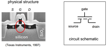
#3This is really fascinating. I apologize if this is a silly question but under the Fabrication section there is a pic titled "physical structure(Texas Instruments, 1997.)" My question is why do all of the components always look so "puffy" or "fuzzy" in these chip zoom-in pics? I guess I'm always surprised that such a precision process produces something with such imperfect looking shapes. Or are these slightly amorphous shapes just a distortion produced by a scanning electron microscope?
EDIT: This is the pic I was asking about: http://sam.zeloof.xyz/wp-content/uploads/2018/04/na_1.png
Re: Home Chip Fab
#4404 :-(
Re: Home Chip Fab
#5404 :-(
Woah, apparently this is because my workplace has added this website to the super-block-without-even-telling-you list...
Re: Home Chip Fab
#6I was at Semicon Japan last year in December and I learn about the coolest semiconductor company (non profit research organization) ever - MinimalFab [1]. There isn't much information their website but this [2] video explains what MinimalFab is about. Essentially, it is a cleanroom-free, modularized fab where each process step in a fab is like a little ATM machine. Miniaturization of complex fab processes is mind blowing and everything is contained inside the machine including a Class 100 environment. Load a tiny quarter sized wafer in a cassette to process and move material from one machine to another. This kind of a fab setup would be incredibly useful to R&D fabs in universities and small scale fabrication for military, space, defense and perhaps even hobby use.
[1] https://www.minimalfab.com/en/ [2] https://www.youtube.com/watch?v=WsOVbmfYxoM
Re: Home Chip Fab
#7Website seems like it got the HN hug of death, archive: https://web.archive.org/web/20190809200012/http://sam.zeloof...
Re: Home Chip Fab
#8I love this! Nanofabrication was one of my favorite classes and even with fancy equipment and worked out ahead of time instructions making a transistor took a huge amount of time and a good number of missteps. Can't imagine the amount of work required to do it all from scratch. Though I also think the safety lectures scared me sufficiently that I wouldn't want to touch HF acid ever again.
Re: Home Chip Fab
#9Re: Home Chip Fab
#10This is really fascinating. I apologize if this is a silly question but under the Fabrication section there is a pic titled "physical structure(Texas Instruments, 1997.)" My question is why do all of the components always look so "puffy" or "fuzzy" in these chip zoom-in pics? I guess I'm always surprised that such a precision process produces something with such imperfect looking shapes. Or are these slightly amorpho…
You're referring to the fact that the edges aren't really sharp and are kind of 'soft', right? Like, everything isn't 90 degree angles and is kinda rippley in places?
If so, that's not an SEM issue, that's just what it looks like. Photo exposure by it's very nature doesn't edge things 100% properly, diffraction or tiny misalignments causes stuff to end up being 'soft'.
Also, keep in mind that was from 1997. Fab tech has gotten way better; although we don't have a scale reference, I imagine if you were to make the same device on modern tech everything would look a lot 'sharper'. You still can't get away from some softness though.