A home-made lithographically-fabricated integrated circuit
1–10 of 122 posts
Re: A home-made lithographically-fabricated integrated circuit
#2Have a mini-course into maskless photolithography[1][2], and find out how an old DLP projector combined with some advanced optics can yield this: http://sam.zeloof.xyz/wp-content/uploads/2017/02/IMG_2917-e1...
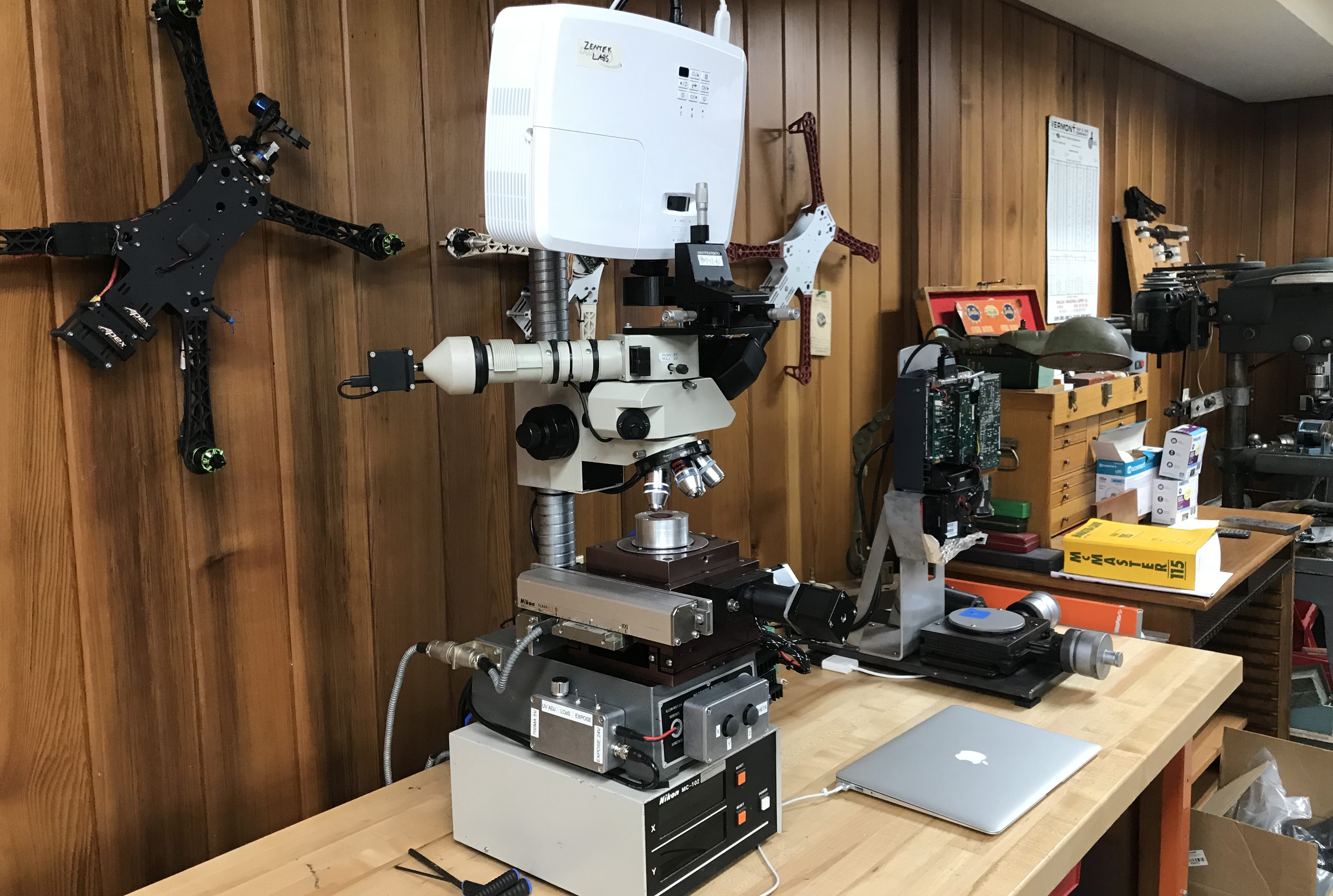
Take a tour in a home fab: https://www.youtube.com/watch?v=TrmqZ0hgAXk
His website and Youtube channel are so richly filled with knowledge that so desperately needs to be in the public domain, instead of being locked in corporate structures.
Re: A home-made lithographically-fabricated integrated circuit
#3OK now grow your own SI wafers using repeated Czochralski process based on silicon you made by melting sand.
Re: A home-made lithographically-fabricated integrated circuit
#4IEEE has a background piece for those (like me) wondering "who is this guy?"
https://spectrum.ieee.org/semiconductors/devices/the-high-sc...
Impressive.
Re: A home-made lithographically-fabricated integrated circuit
#5OK now grow your own SI wafers using repeated Czochralski process based on silicon you made by melting sand.
This seems to be a little silly. Sure, that'd be cool, but I mean, he didn't claim to have manufactured his own oscilloscopes here either.
Re: A home-made lithographically-fabricated integrated circuit
#6OK now grow your own SI wafers using repeated Czochralski process based on silicon you made by melting sand.
This seems to be a little silly. Sure, that'd be cool, but I mean, he didn't claim to have manufactured his own oscilloscopes here either.
Just putting out next step learning challenges. I'm loving what he's doing, it's a great project, I hope he continues it by exploring different aspects of it.
Other challenges include smaller lithography and CMOS fabrication using a self-aligned gate process. But there are pitfalls ahead, including chemicals that can kill with in trace doses...
I fabricated my own ICs as a teen in my freshman year of college as part of our program, but that obviously wasn't at home. It was still awesome, just going through the entire process.
Re: A home-made lithographically-fabricated integrated circuit
#7OK now grow your own SI wafers using repeated Czochralski process based on silicon you made by melting sand.
You just can't impress everyone.
Re: A home-made lithographically-fabricated integrated circuit
#8OK now grow your own SI wafers using repeated Czochralski process based on silicon you made by melting sand.
[deleted]
Re: A home-made lithographically-fabricated integrated circuit
#9I was looking for how he managed the clean room or did he not go too small. Found the answer in the IEEE article shared by another commenter (he didn't go below 10 micron tech node).
But now I have a follow up question, if getting a clean room is obviously harder, isn't "clean box" more doable? E.g., if you line up a bunch of tables, and put a long box on top that acts like a poor man's assembly line. The insides of that box are only accessible through gloves that are attached to holes on the sides of the box, and plenty of glass windows to look inside (kinda like the box in movie 'Life'). How cost effective and feasible (i.e., gets the job done) would that be compared to a clean room? maybe you could go sub-micron with it if not sub-100nm.
Re: A home-made lithographically-fabricated integrated circuit
#10Impressive to replicate silicon semiconductor process.
But wouldn't it be more feasible to develop as good enough process node, flexible, thin film semiconductor devices?
Have been observing developments of plastic based transistors, inks, processes like nanoimprint lithography,
Cleanroom in a STEM microscope and Chad Mirkin's Tera Print system.
Can a small scale nanfab emerge using tech such as Nano-Ops http://nano-ops.net/nanoscale-printing/ ?
I imagine flexible, thin film, large panel based semiconductor SoC. It will not be just a mere microcontroller or IoT node, but a full fleged computing form factor. Think your wall as big plastic computer.