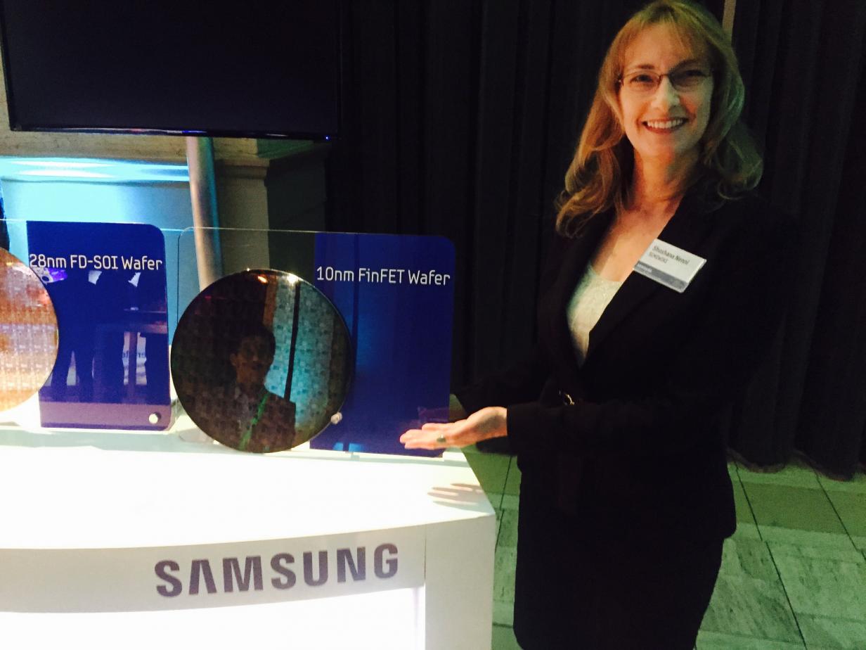
There isn't any feature of the transistors taht are 7nm wide, the smallest feature IIRC is the interconnect, which is about 30n-40nm. "7nm" is marketing wankery. https://en.wikichip.org/wiki/7_nm_lithography_process
Well that's annoying. How is anyone supposed to judge anything if they just make numbers up?
Well, after a while or is sort of public knowledge that 10nm Intel is about the same as 12nm AMD, etc.
But yes, the industry needs standardized advertising practices badly.
Wow. I still remember being amazed when micron widths came out. 7nm is close to a miracle. Semiconductor manufacturing improvements like this really have enabled the whole tech world improvements of the last few decades.
There isn't any feature of the transistors taht are 7nm wide, the smallest feature IIRC is the interconnect, which is about 30n-40nm. "7nm" is marketing wankery. https://en.wikichip.org/wiki/7_nm_lithography_process
If you look at the SRAM bit cells, they halved in area from 28nm to 14nm, and halved again from 14nm to 7nm. This is likely due to metal interconnects or other features only halving in spacing going from 28nm process to 7nm. So the scaling almost appears to apply to only one dimension (full linear scaling of two dimensions would have quartered the cell area at each step resulting in a 16-fold total reduction). But it is still scaling nevertheless.
Wow. I still remember being amazed when micron widths came out. 7nm is close to a miracle. Semiconductor manufacturing improvements like this really have enabled the whole tech world improvements of the last few decades.
There isn't any feature of the transistors taht are 7nm wide, the smallest feature IIRC is the interconnect, which is about 30n-40nm. "7nm" is marketing wankery. https://en.wikichip.org/wiki/7_nm_lithography_process
There are different features sizes in the Z direction and different feature sizes in the XY plane. When it comes to XY, the smallest features size is probably the gate length. When it comes to Z, the gate oxide width is probably the smallest at 1-2nm. We have something called atomic layer deposition which gives control over single atomic layer thicknesses.
Fun stuff. I've got a key chain with an 80186 die, and a couple of the binders from Microprocessor Forum when they had dies on the cover. The features on those chips are "huge" compared to these things. I suspect a die using one of these processes that was big enough (say 100 sq mm) would just look like a mirror with chromatic interference lines running across it. This announcement also bookends nicely with the first…
ICs have just looked like mirrors for a while now. See this shot of a 14nm Vega die on the left and 28nm Fury die on the right: https://www.techpowerup.com/reviews/AMD/Radeon_RX_Vega_Previ...
I think you linked to a flip chip---you would expect a mirror finish from the bulk silicon side.
Fun stuff. I've got a key chain with an 80186 die, and a couple of the binders from Microprocessor Forum when they had dies on the cover. The features on those chips are "huge" compared to these things. I suspect a die using one of these processes that was big enough (say 100 sq mm) would just look like a mirror with chromatic interference lines running across it. This announcement also bookends nicely with the first…
Wow. I still remember being amazed when micron widths came out. 7nm is close to a miracle. Semiconductor manufacturing improvements like this really have enabled the whole tech world improvements of the last few decades.
There isn't any feature of the transistors taht are 7nm wide, the smallest feature IIRC is the interconnect, which is about 30n-40nm. "7nm" is marketing wankery. https://en.wikichip.org/wiki/7_nm_lithography_process
I've always assumed that "XX nm" doesn't represent the geometry of any particular feature of the end product, but something related to the wavelength of the radiation used for the imaging process.
Maybe it corresponds to the principle emission line of the light source (synchrotron?) In spectral terms, 7 nm is near the border between hard UV radiation and soft X-rays.