Live data from Hacker News

New Transistor Structures At 3nm/2nm

semiengineering.com

21–30 of 82 posts

Re: New Transistor Structures At 3nm/2nm

#21

What is the benefit of smaller transistors? Serious question. Why does it matter if I have 7nm vs. 5nm vs. anything else?

The marginal cost of manufacturing a chip is roughly proportional to area. So with smaller transistors you can fit more of them into a given area.

Re: New Transistor Structures At 3nm/2nm

#22

What is the benefit of smaller transistors? Serious question. Why does it matter if I have 7nm vs. 5nm vs. anything else?

It's crazy to think about if you've never thought about this, but the speed of light is a bottleneck for processors. When we get smaller devices, there's literally less distance that needs to be traversed, so more can be done!

Re: New Transistor Structures At 3nm/2nm

#23
post #9
post #2

This drawing is a bit clearer and more complete than the one in the article: https://images.anandtech.com/doci/16041/SamGAA_575px.png Note that "MBCFET" is Samsung's name for their "nanosheet" FET. And the Anandtech article it comes from: https://www.anandtech.com/show/16041/where-are-my-gaafets-ts...

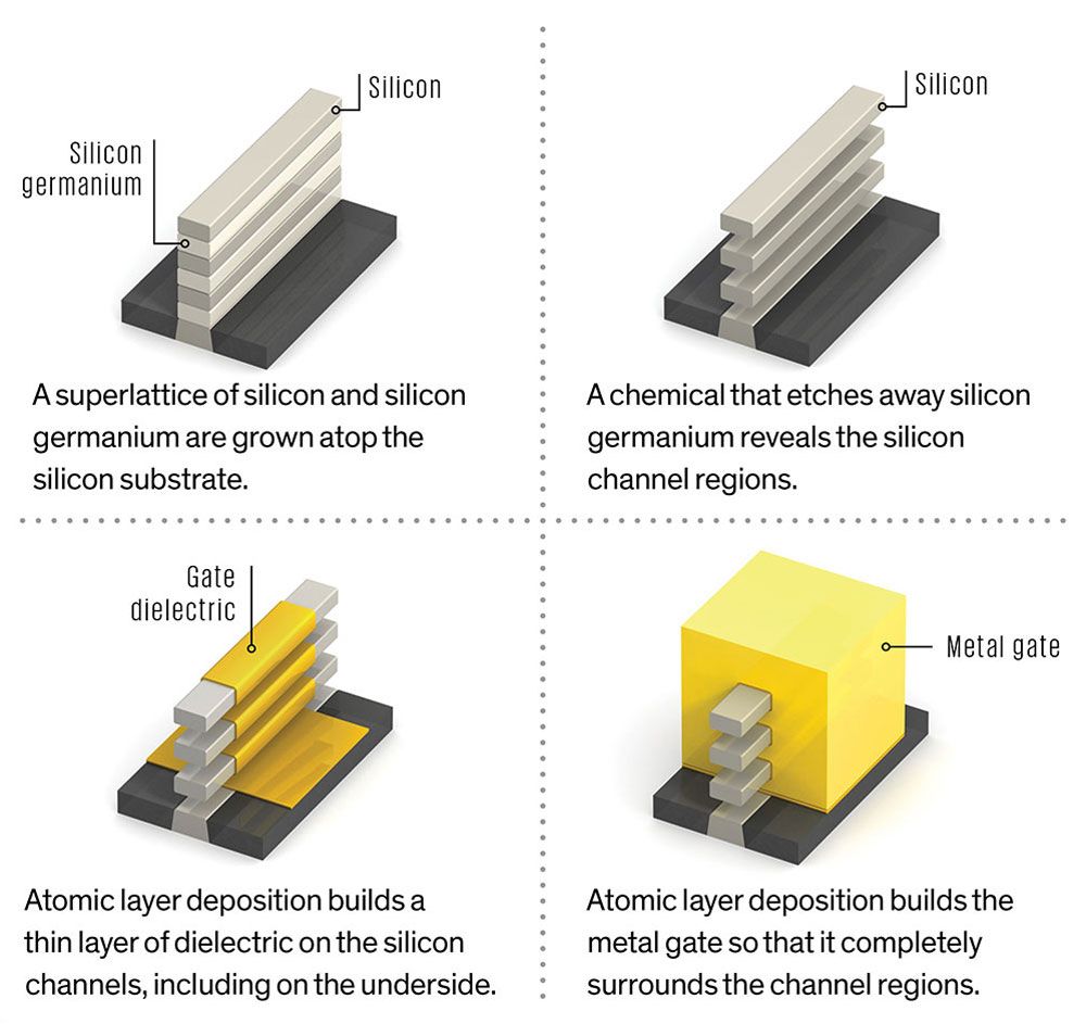
Are there drawings with more detail? I'm unclear where the gate dielectric is and the channel. The silicon is doped differently "inside" the gate to form the channel? That seems hard to fabricate. (I searched around a bit but couldn't find a better diagram.)

This diagram seems to be what you're looking for: https://spectrum.ieee.org/image/MzM0NTY3NA.jpeg

Shows the stages of material removal/deposit so that the dielectric and channel are clear.

Re: New Transistor Structures At 3nm/2nm

#24

What is the benefit of smaller transistors? Serious question. Why does it matter if I have 7nm vs. 5nm vs. anything else?

Smaller distance -> lower resistance -> less heat -> higher clocks/more stuff per clock allowed with same amount of heat produced -> higher performance.

No smaller dimensions -> thinner wires -> higher resistance per length.

Re: New Transistor Structures At 3nm/2nm

#25
post #21

What is the benefit of smaller transistors? Serious question. Why does it matter if I have 7nm vs. 5nm vs. anything else?

The marginal cost of manufacturing a chip is roughly proportional to area. So with smaller transistors you can fit more of them into a given area.

Exactly, the smaller your chip is the more you can fit on a silicon wafer.

If your chip is too large it can even make it practically impossible to manufacture at scale due to the increased chance of defects as your chip size increases.

Re: New Transistor Structures At 3nm/2nm

#26

What is the benefit of smaller transistors? Serious question. Why does it matter if I have 7nm vs. 5nm vs. anything else?

It's crazy to think about if you've never thought about this, but the speed of light is a bottleneck for processors. When we get smaller devices, there's literally less distance that needs to be traversed, so more can be done!

> the speed of light is a bottleneck for processors

It's not the speed of light [in a vacuum], but electric signal propagation speed in copper.

Re: New Transistor Structures At 3nm/2nm

#27

What is the benefit of smaller transistors? Serious question. Why does it matter if I have 7nm vs. 5nm vs. anything else?

It's crazy to think about if you've never thought about this, but the speed of light is a bottleneck for processors. When we get smaller devices, there's literally less distance that needs to be traversed, so more can be done!

this is only true because diodes are not superconductors, and even if the traveling distance is small, the joule effect is significant.

Re: New Transistor Structures At 3nm/2nm

#28
One thing I've always wondered about when it comes to new process design at smaller scale: how much actual quantum mechanics is actually needed to get the job done?

And ... if the answer is, as I suspect, a lot, what kind of numerical methods and processes are used to design and simulate these tiny quantum mechanical machines?

[EDIT] I mean, when taking a basic QM course, there is a lot of contorsions to try and find analytical solutions to the Schrödinger equation, but as soon as you have three particle interacting with each other, analytical methods run into a wall.

Am I right to think that sub-10nm process design is all done numerically?

Anyone who happens to work on this type of problems care to give pointers?
Re: New Transistor Structures At 3nm/2nm

#29

What is the benefit of smaller transistors? Serious question. Why does it matter if I have 7nm vs. 5nm vs. anything else?

Smaller means closer together. Closer together means less time for a signal to move from one to another. Less time means higher clock speeds. If you CPU is 100mm across, the speed of light limits it to 3GHz because that's how many times you can cross the cpu travelling at c. At 10mm you get 30GHz.

I don't really know enough to refute it, but this seems deeply and bizarrely wrong. It doesn't account for transistor count or density just the size of the entire chip? With pipelining I don't think a signal has to travel across the entire chip every cycle. It also doesn't really address the question above, since single core CPU speeds haven't increased in 15 years even though transistors have kept getting smaller and closer together.

Seems like an intriguing napkin math limit/simplification though, I'd be interested if anyone could elaborate on if there's any substance to it.

Re: New Transistor Structures At 3nm/2nm

#30

Silicon atoms are about 0.13nm apart. 2nm is about 15 atoms wide. Mass producing anything on that scale is an exceptional feat.

It's been a while since node names were actually physical measurements though. For example, at the 3nm node the fin width is 5nm (as noted in the article).
Post reply on HN