Live data from Hacker News

Teardown: Identifying Apple M1's distinct circuit blocks

eetasia.com

11–20 of 27 posts

Re: Teardown: Identifying Apple M1's distinct circuit blocks

#11

Are there any home made methods to take picture of the chips like this? What tools would you use to sand the top of the chip? What type of microscope would work?

To get the die off the flip chip carrier I use heat and scraping. Then I use a razor blade to scrape off most of the metal layers (which obscure the functional blocks), then a cheap Chinese inspection microscope ($100) attached to a DSLR with a 3D printed adapter (a DSLR with a lens attached backwards also works in a pinch). Then take a bunch of individual photos and stitch them with Hugin.

Results: https://marcan.st/transf/latte_stitched.jpg
Edit: sorry, the link was previously the (lower res!) Chipworks shot I'd annotated previously. I got confused. Replaced with mine. It's less clean but higher resolution than what they released.

At the highest zoom I could get I could just about make out individual bits in the eFuse array. This is a Wii U GPU (Latte).

https://marcan.st/transf/latte_otp_slr.jpg
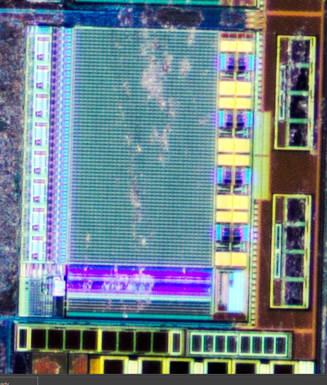
No chemicals needed. I'm probably one of very few people crazy enough to do this mechanically, but it clearly works!

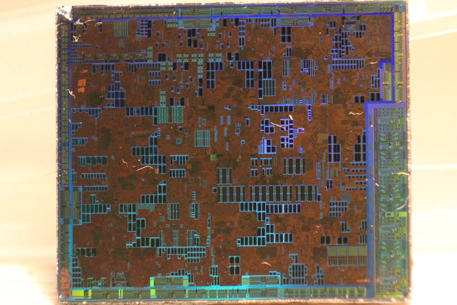
Here's a single shot done with a reversed cheap kit Canon lens of a PS3 GPU (RSX), again with the scraping method.

https://marcan.st/transf/rsx.jpg
I do happen to have access to a SEM too, and obviously that gets a lot more fun. Here's the same eFuse area (again this is still the mechanically deprocessed chip!):

https://marcan.st/transf/sem/latte/20161210_201044.png
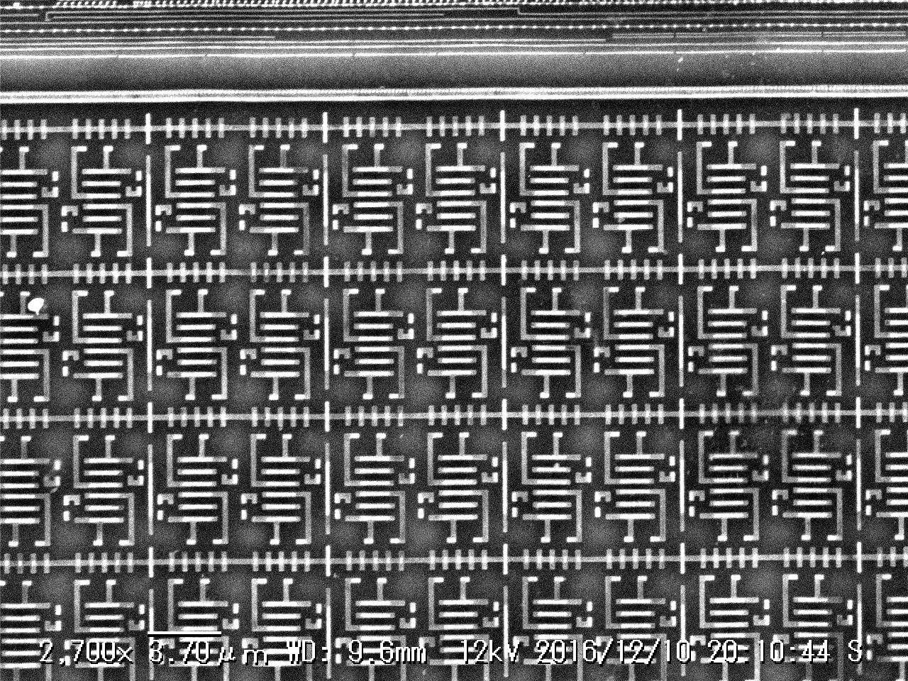
I think the mechanical delayering usually gets me to M1 or so, though it's not completely consistent depending on the specific process. Some chips work better than others.

Re: Teardown: Identifying Apple M1's distinct circuit blocks

#12
post #4
post #2

This article does not appear to do what the title claims. It mostly rounds up news from other sources. Has anyone done the actual analysis of what the dedicated logic cores on the M1 are? I'm always curious what kinds of work Apple dedicates hardware to.

Is it really possible to get such analysis if you're not a macos developer? From a layman point of view, I would take a list of instructions executed during common case OS usage and then extract the most common patterns (basically compression) and put them into silicon. These wouldn't be easy to understand if you don't know exactly what the OS is doing and how. I mean of course you need some cleanup and well thought-…

They actually did this in the M1 for retain/release for Objective-C and Swift objects. It's an extremely common operation on the platform and is 4x faster on M1 natively, and still 2x faster than native Intel under Rosetta.

Re: Teardown: Identifying Apple M1's distinct circuit blocks

#13
post #4

Earlier quoted context omitted.

Is it really possible to get such analysis if you're not a macos developer? From a layman point of view, I would take a list of instructions executed during common case OS usage and then extract the most common patterns (basically compression) and put them into silicon. These wouldn't be easy to understand if you don't know exactly what the OS is doing and how. I mean of course you need some cleanup and well thought-…

"There are no secrets in silicon" A determined enough team of people with sulfuric acid and electron microscopes could work out exactly what is going on inside the chip. (not that anyone would actually do this - maybe Intel? But at least in principle, the information is accessible to non-Apple folks)

We do. This is what we have publicly disclosed about our findings thus far. https://www.techinsights.com/blog/two-new-apple-socs-two-mar...

Re: Teardown: Identifying Apple M1's distinct circuit blocks

#14

Earlier quoted context omitted.

"There are no secrets in silicon" A determined enough team of people with sulfuric acid and electron microscopes could work out exactly what is going on inside the chip. (not that anyone would actually do this - maybe Intel? But at least in principle, the information is accessible to non-Apple folks)

We do. This is what we have publicly disclosed about our findings thus far. https://www.techinsights.com/blog/two-new-apple-socs-two-mar...

Is it common to put fake features in silicon to make reverse engineering harder?

Re: Teardown: Identifying Apple M1's distinct circuit blocks

#15
post #4
post #2

This article does not appear to do what the title claims. It mostly rounds up news from other sources. Has anyone done the actual analysis of what the dedicated logic cores on the M1 are? I'm always curious what kinds of work Apple dedicates hardware to.

Is it really possible to get such analysis if you're not a macos developer? From a layman point of view, I would take a list of instructions executed during common case OS usage and then extract the most common patterns (basically compression) and put them into silicon. These wouldn't be easy to understand if you don't know exactly what the OS is doing and how. I mean of course you need some cleanup and well thought-…

This is effectively what happens anyway because the CPU manufacturers beat each other over the head with various benchmarks, but it's worth saying that very little area of a modern CPU is actually taken up by functional units like adders

Re: Teardown: Identifying Apple M1's distinct circuit blocks

#16
post #14

Earlier quoted context omitted.

We do. This is what we have publicly disclosed about our findings thus far. https://www.techinsights.com/blog/two-new-apple-socs-two-mar...

Is it common to put fake features in silicon to make reverse engineering harder?

Not really (that i have seen). I am not an analyst though, so not a guarantee. Die real estate is extremely expensive. Plus it wouldn’t really throw us off the scent due to the techniques we employ.

Re: Teardown: Identifying Apple M1's distinct circuit blocks

#17

Are there any home made methods to take picture of the chips like this? What tools would you use to sand the top of the chip? What type of microscope would work?

To get the die off the flip chip carrier I use heat and scraping. Then I use a razor blade to scrape off most of the metal layers (which obscure the functional blocks), then a cheap Chinese inspection microscope ($100) attached to a DSLR with a 3D printed adapter (a DSLR with a lens attached backwards also works in a pinch). Then take a bunch of individual photos and stitch them with Hugin. Results: https://marcan.st…

This is really cool, thanks for sharing

Re: Teardown: Identifying Apple M1's distinct circuit blocks

#18
I'm not sure what to make of that Neural Engine. I was under the impression that most machine learning was using GPUs. The M1 already has a large GPU, so I'm surprised that the chip developers decided that a dedicated neural processor was worthwhile, especially in the middle of those CPUs.

Also, what kinds of jobs is that neural engine for? Presumably voice and face recognition to start with, but that doesn't strike me as enough to justify that die space. Good for research of course, but Apple seems to focus on what's practical for everyday users. I've seen stories about CPU designers wanting to use machine learning to manage system cache. I wonder if the NPU will be involved in managing the workload of the M1 chip itself.

Re: Teardown: Identifying Apple M1's distinct circuit blocks

#19
post #18

I'm not sure what to make of that Neural Engine. I was under the impression that most machine learning was using GPUs. The M1 already has a large GPU, so I'm surprised that the chip developers decided that a dedicated neural processor was worthwhile, especially in the middle of those CPUs. Also, what kinds of jobs is that neural engine for? Presumably voice and face recognition to start with, but that doesn't strike…

It’s an interesting question. For one, I know that the Photos app on Macs and iPhones tends to spend loads of time going through your photos and recognizing everyone’s faces. Due to Apple’s stance on privacy, they’ve emphasized that this task should be performed on device, not in the cloud.

Without the neural engine, the processing of tens of thousands of photos can be a real burden on a typical MacBook. Apple has tried to throttle the process so that it doesn’t peg the CPU, but then it takes a lot longer to complete. The neural engine lets the process run full out without consuming a ton of power.

Re: Teardown: Identifying Apple M1's distinct circuit blocks

#20
post #18

I'm not sure what to make of that Neural Engine. I was under the impression that most machine learning was using GPUs. The M1 already has a large GPU, so I'm surprised that the chip developers decided that a dedicated neural processor was worthwhile, especially in the middle of those CPUs. Also, what kinds of jobs is that neural engine for? Presumably voice and face recognition to start with, but that doesn't strike…

It is also used for Siri, for automatically making albums for Photos, finding people in Photos.

I think the NPU is not as power hungry for inference than the GPU is for the same job.

Post reply on HN