Earlier quoted context omitted.
Two 16 KiB ROMs, actually. (Meanwhile, current Intel processors have 2 MiB microcode files.)
to be fair, that's 2 MiB code that is the base of the other os you never heard of, the IME, AMT and their backdoor capabilities [1] 1: https://fsf.org/blogs/community/active-management-technology
Nibbler 4 Bit CPU
11–20 of 20 posts
Re: Nibbler 4 Bit CPU
#12Nibbler also lacks any address registers, which means it can’t support any form of indirect addressing, nor a hardware-controlled stack. All memory references must use absolute addresses. Wow!
Yes, it is a very limited design, but the thought, that it was implemented just using (very few!) standard 74xxx TTL logic is really amazing. And still it runs with 1MHz, the same speed of my first computer ;) with a dedicated integrated CPU.
Re: Nibbler 4 Bit CPU
#13Nibbler also lacks any address registers, which means it can’t support any form of indirect addressing, nor a hardware-controlled stack. All memory references must use absolute addresses. Wow!
[] Indirect addressing was an optional feature on the IBM 1401 for an additional monthly fee.
On the topic of processors made from 74xx TTL, I'll point out the Datapoint 2200 desktop computer. This had a board of TTL chips equivalent to the 8008 microprocessor. The 8008 was actually designed to replace this TTL-based processor. Trivia: the x86 is little-endian because when building a serial computer from TTL it's easier to use little-endian. https://en.wikipedia.org/wiki/Datapoint_2200
The Nibbler is different from the PDP, Datapoint, etc in that the Nibbler has very, very few chips; almost all the logic is done in microcode. This is the same trick used to build a "single-chip" processor from the Four Phase AL1. https://en.wikipedia.org/wiki/Four-Phase_Systems
Re: Nibbler 4 Bit CPU
#14Earlier quoted context omitted.
The ROM is basically acting as an FPGA. After all, an FPGA is just a load of units of small ROM areas, with the inputs and outputs linked to each other. If all you need to implement your circuit is a single unit, then a small ROM chip is quite sufficient instead.
> The ROM is basically acting as an FPGA. No, it doesn't; neither from a practical, nor from a theoretical point of view. Theoretically, ROMs are equivalent to the class of pure, total, mathematical functions (i.e., each input value maps to exactly one output value), while FPGAs are equivalent to the class of deterministic finite automata, because they contain internal state. > After all, an FPGA is just a load of un…
I'd argue that an even more critical feature of FPGAs is configurable routing. ROMs don't have that either. :)
Re: Nibbler 4 Bit CPU
#15Earlier quoted context omitted.
Yes, it is a very limited design, but the thought, that it was implemented just using (very few!) standard 74xxx TTL logic is really amazing. And still it runs with 1MHz, the same speed of my first computer ;) with a dedicated integrated CPU.
I have a 12 bit CPU at home that is implemented out of standard 74xxx TTL chips, its called a PDP-8/e :-). Not to take away from the Nibbler design, its great, but using TTL logic to build CPUs was a thing for a pretty long period of time (computer wise), probably 10 years from 1971 - 1981. 1981 was the year IBM introduced the IBM PC and a lot of people realized that bespoke CPU architectures were a luxury they could…
I guess, the PDP has at least 10 times more (equivalent) chips inside.
Re: Nibbler 4 Bit CPU
#16Earlier quoted context omitted.
I have a 12 bit CPU at home that is implemented out of standard 74xxx TTL chips, its called a PDP-8/e :-). Not to take away from the Nibbler design, its great, but using TTL logic to build CPUs was a thing for a pretty long period of time (computer wise), probably 10 years from 1971 - 1981. 1981 was the year IBM introduced the IBM PC and a lot of people realized that bespoke CPU architectures were a luxury they could…
Of course the technique itself is not that new, but it is still amazing, because of the real few chips used. Of course the microcode ROM replaces plenty of those, but still it amazes me, how few chips make up for a workable CPU. I guess, the PDP has at least 10 times more (equivalent) chips inside.
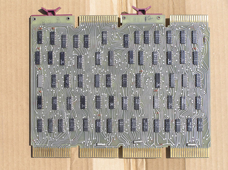
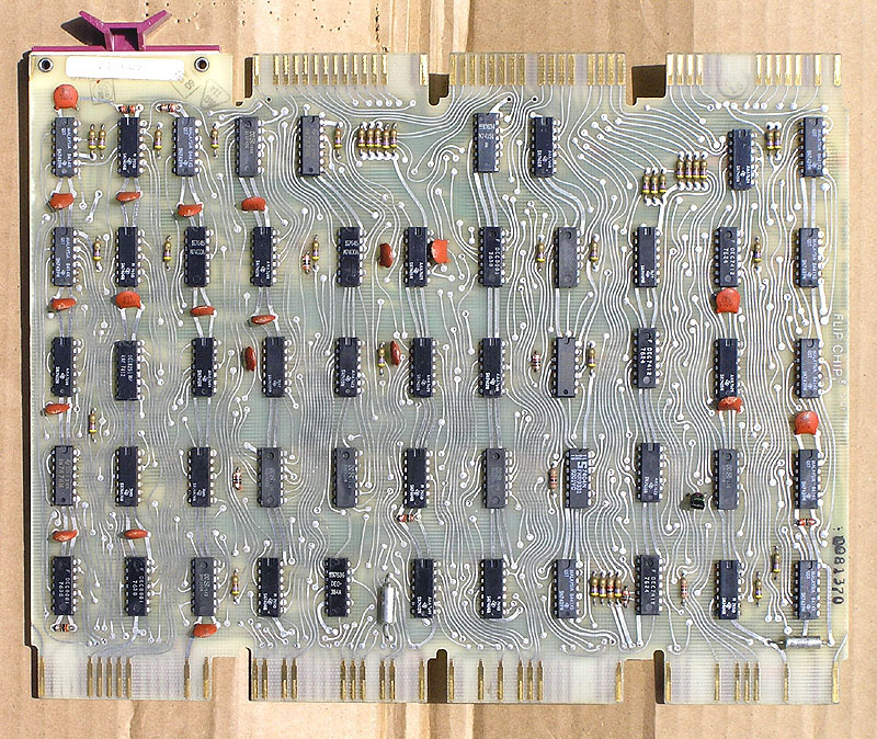
M8310 - 53 chips (http://www.classiccmp.org/hp/My%20PDP-8%20Cards/M8310.jpg)
M8300 - 64 chips (http://www.classiccmp.org/hp/My%20PDP-8%20Cards/M8300.jpg)
So 117 chips, so not quite 10X but the nibbler does have an LCD display and if you add the PDP-8/e programmer console to the mix you're probably close to 170 chips. So great estimate!
Re: Nibbler 4 Bit CPU
#17Earlier quoted context omitted.
> The ROM is basically acting as an FPGA. No, it doesn't; neither from a practical, nor from a theoretical point of view. Theoretically, ROMs are equivalent to the class of pure, total, mathematical functions (i.e., each input value maps to exactly one output value), while FPGAs are equivalent to the class of deterministic finite automata, because they contain internal state. > After all, an FPGA is just a load of un…
> You're forgetting the memory elements – they're crucial to the functionality of FPGAs. I'd argue that an even more critical feature of FPGAs is configurable routing. ROMs don't have that either. :)
Re: Nibbler 4 Bit CPU
#18Earlier quoted context omitted.
> You're forgetting the memory elements – they're crucial to the functionality of FPGAs. I'd argue that an even more critical feature of FPGAs is configurable routing. ROMs don't have that either. :)
True. But then again, that's like arguing over which organ is more important – the heart or the lung – when you can't survive without either of them ;-)
Actually, now I wonder whether it'd be possible to build memory out of ROM by looping outputs back to inputs...
Re: Nibbler 4 Bit CPU
#19Earlier quoted context omitted.
True. But then again, that's like arguing over which organ is more important – the heart or the lung – when you can't survive without either of them ;-)
You can build memory elements - inefficiently, but it's possible - out of recurrent logic. You can't build routing. Actually, now I wonder whether it'd be possible to build memory out of ROM by looping outputs back to inputs...
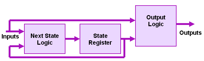
You actually don't need configurable (programmable) routing: We can model every synchronous circuit as a Mealy machine [1], therefore we need two functions and a register. Every function can be constructed from a hierarchy of programmable, fixed-size LUTs which are statically connected (for example, you can build a 5-input LUT from three 4-input LUTs). Now you don't need to build routing, it's implicit in the next-state and output functions.
[1] like this: http://electrosofts.com/verilog/mealy.gif
Re: Nibbler 4 Bit CPU
#20Earlier quoted context omitted.
to be fair, that's 2 MiB code that is the base of the other os you never heard of, the IME, AMT and their backdoor capabilities [1] 1: https://fsf.org/blogs/community/active-management-technology
No, that's just the CPU µcode. IME/AMT are part of the BIOS/EFI images, which is a whopping 16 MiB for my current motherboard.