New Transistor Structures At 3nm/2nm
semiengineering.com
New Transistor Structures At 3nm/2nm
1–10 of 82 posts
Re: New Transistor Structures At 3nm/2nm
#2This drawing is a bit clearer and more complete than the one in the article: https://images.anandtech.com/doci/16041/SamGAA_575px.png
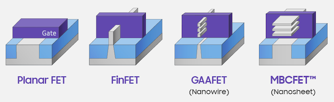
Note that "MBCFET" is Samsung's name for their "nanosheet" FET.
And the Anandtech article it comes from: https://www.anandtech.com/show/16041/where-are-my-gaafets-ts...
Re: New Transistor Structures At 3nm/2nm
#3Rather than the change in transistor design, I think the bigger news is the switch from silicon with dopants to silicon with germanium and dopants. The drop in threshold voltage from ~0.7v to ~0.3v might be one of the last levers left in extracting even more performance; at the cost of making semi production and equipment even more hazardous.
Re: New Transistor Structures At 3nm/2nm
#4Rather than the change in transistor design, I think the bigger news is the switch from silicon with dopants to silicon with germanium and dopants. The drop in threshold voltage from ~0.7v to ~0.3v might be one of the last levers left in extracting even more performance; at the cost of making semi production and equipment even more hazardous.
Would you mind explaining how the production becomes more hazardous?
Re: New Transistor Structures At 3nm/2nm
#5Another good resource for moving to GAA FETs https://semiengineering.com/moving-to-gaa-fets/
Re: New Transistor Structures At 3nm/2nm
#6Rather than the change in transistor design, I think the bigger news is the switch from silicon with dopants to silicon with germanium and dopants. The drop in threshold voltage from ~0.7v to ~0.3v might be one of the last levers left in extracting even more performance; at the cost of making semi production and equipment even more hazardous.
What do you mean "silicon with germanium and dopants"? Implanting germanium as a dopant is already done at much larger geometries than 2/3nm. It's also not any more hazardous than implanting any other ion.
Re: New Transistor Structures At 3nm/2nm
#7Rather than the change in transistor design, I think the bigger news is the switch from silicon with dopants to silicon with germanium and dopants. The drop in threshold voltage from ~0.7v to ~0.3v might be one of the last levers left in extracting even more performance; at the cost of making semi production and equipment even more hazardous.
Would you mind explaining how the production becomes more hazardous?
I think parent might have confused Germanium with Cadmium? I am no chemist. It could also require other more toxic substances to control reactions or act a carrier. The whole area around Sunnyvale is littered with toxic waste dumps from semiconductor manufacturing. [1] From [2], it says, "Some reactive intermediate compounds of germanium are poisonous", when then references [3] but I can't find the specific citation. I think Germanium is getting lumped in with other toxic chemicals used in semiconductor manufacturing like gallium arsenide, cadmium, etc.
[1] https://www.epa.gov/superfund-redevelopment-initiative/super...
[2] https://en.wikipedia.org/wiki/Germanium#Germanium_and_health
[3] https://www.usgs.gov/centers/nmic/germanium-statistics-and-i...
https://pubchem.ncbi.nlm.nih.gov/compound/germanium#section=...
https://pubchem.ncbi.nlm.nih.gov/compound/cadmium#section=To...
Re: New Transistor Structures At 3nm/2nm
#8Rather than the change in transistor design, I think the bigger news is the switch from silicon with dopants to silicon with germanium and dopants. The drop in threshold voltage from ~0.7v to ~0.3v might be one of the last levers left in extracting even more performance; at the cost of making semi production and equipment even more hazardous.
According to the article, the new transistor design offers the promise of lower leakage.
Re: New Transistor Structures At 3nm/2nm
#9This drawing is a bit clearer and more complete than the one in the article: https://images.anandtech.com/doci/16041/SamGAA_575px.png Note that "MBCFET" is Samsung's name for their "nanosheet" FET. And the Anandtech article it comes from: https://www.anandtech.com/show/16041/where-are-my-gaafets-ts...
Are there drawings with more detail? I'm unclear where the gate dielectric is and the channel. The silicon is doped differently "inside" the gate to form the channel? That seems hard to fabricate. (I searched around a bit but couldn't find a better diagram.)
Re: New Transistor Structures At 3nm/2nm
#10What is the benefit of smaller transistors? Serious question. Why does it matter if I have 7nm vs. 5nm vs. anything else?